Band Gap Tuning of Solution-Processed Ferroelectric Perovskite BiFe1–xCoxO3 Thin Films

Pamela MachadoMateusz ScigajJaume GazquezEstel RuedaAntonio Sánchez-DíazIgnasi FinaMartí Gibert-RocaTeresa PuigXavier ObradorsMariano Campoy-Quiles, and Mariona Coll*Chem. Mater.201931 (3), pp 947–954  DOI: 10.1021/acs.chemmater.8b04380

Ferroelectric perovskite oxides are emerging as a promising photoactive layer for photovoltaic applications because of their very high stability and their alternative ferroelectricity-related mechanism for solar energy conversion that could lead to extraordinarily high efficiencies. One of the biggest challenges so far is to reduce their band gap toward the visible region while simultaneously retaining ferroelectricity. To address these two issues, herein an elemental composition engineering of BiFeO3 is performed by substituting Fe by Co cations, as a means to tune the characteristics of the transition metal–oxygen bond. We demonstrate by solution processing the formation of epitaxial, pure phase, and stable BiFe1–xCoxO3 thin films for x ≤ 0.3 and film thickness up to 100 nm. Importantly, the band gap can be tuned from 2.7 to 2.3 eV upon cobalt substitution while simultaneously enhancing ferroelectricity. As a proof of concept, nonoptimized vertical devices have been fabricated and, reassuringly, the electrical photoresponse in the visible region of the Co-substituted phase is improved with respect to the unsubstituted oxide.

Direct and Converse Piezoelectric Responses at the Nanoscale from Epitaxial BiFeO3 Thin Films Grown by Polymer Assisted Deposition

DOI:10.1039/C8NR05737K

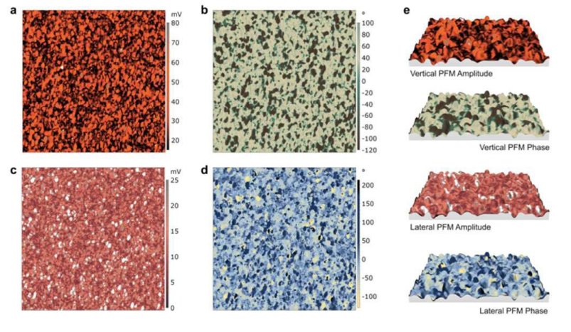
We use an original water-based chemical method, to grow pure epitaxial BiFeO3 (BFO) ultra-thin films with excellent piezoelectric properties. Particularly, we show that this novel chemical route produces a higher natural ferroelectric domain size distribution and coercive field compared to similar BFO films grown by physical methods. Moreover, we measured the d33 piezoelectric coefficient of 60 nm thick BFO films with a direct approach, using Direct Piezoelectric Force Microscopy (DPFM). As a result, first piezo-generated charge maps of a very thin BFO layer were obtained applying this novel technology. We also performed a comparative study of the d33 coefficients between standard PFM analysis and the DPFM microscopy showing similar values i.e. 17 pm/V and 22 pC/N respectively. Finally, we proved that the directionality of the piezoelectric effect in BFO ferroelectric thin films is preserved at low thickness dimensions demonstrating the potential of chemical processes for the development of low cost functional ferroelectric and piezoelectric devices.

Defect landscape and electrical properties in solution-derived LaNiO3 and NdNiO3 epitaxial thin films

B. Mundet, J. Jareño, J. Gazquez, M. Varela, X. Obradors, and T. Puig. Phys. Rev. Materials 2, 063607 

DOI:https://doi.org/10.1103/PhysRevMaterials.2.063607

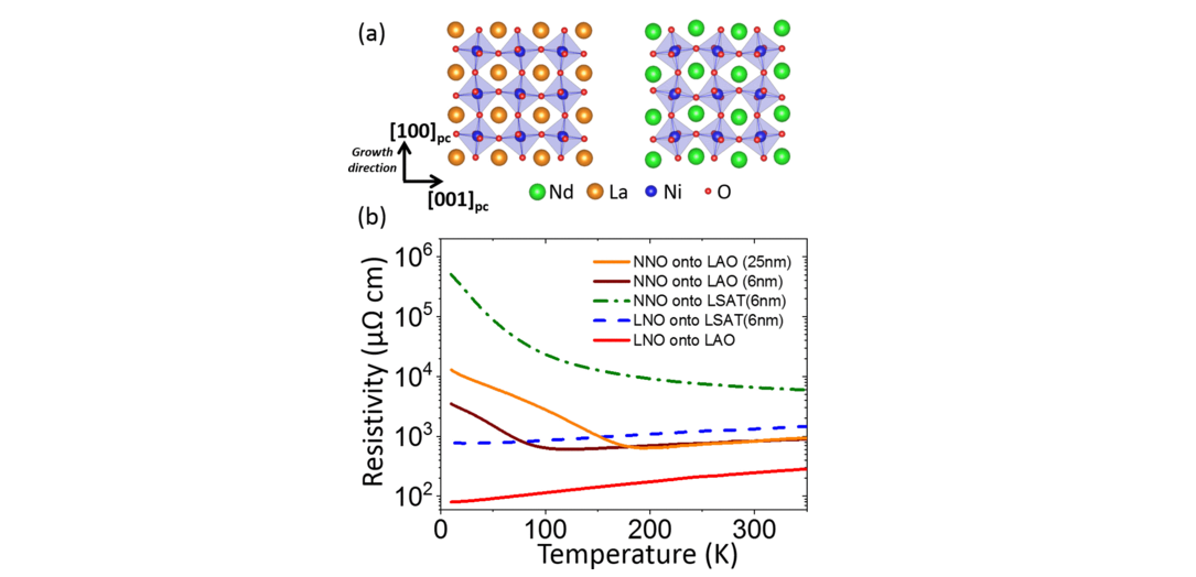
In this work we evaluate the defects and the associated distortions present in tensile and compressive-strained chemical solution deposition–derived NdNiO3 (NNO) and LaNiO3 (LNO) thin films by means of aberration corrected scanning transmission electron microscopy. We elucidate a fundamental link between strain and the most common defect observed in nickelate films, the Ruddlesden-Popper fault (RPF), which will ultimately impinge on the electrical properties of the films. Overall, the concentration of RPF defects increases with the lattice mismatch. More specifically, LNO films are always metallic, although transitioning from compressive to tensile strain results in the appearance of RPFs and an increase of the resistivity. On the other hand, NNO films always behave as insulators under tensile strain, whereas under compressive strain the increase of the thickness makes the onset of the metal-to-insulator transition shift to higher temperatures.

Piezo-generated charge mapping revealed through direct piezoelectric force microscopy

Piezo-generated charge mapping revealed through direct piezoelectric force microscopy

A. GomezM. GichA. Carretero-GenevrierT. Puig & X. Obradors Nature Communications 8, Article number: 1113 (2017) doi:10.1038/s41467-017-01361-2 

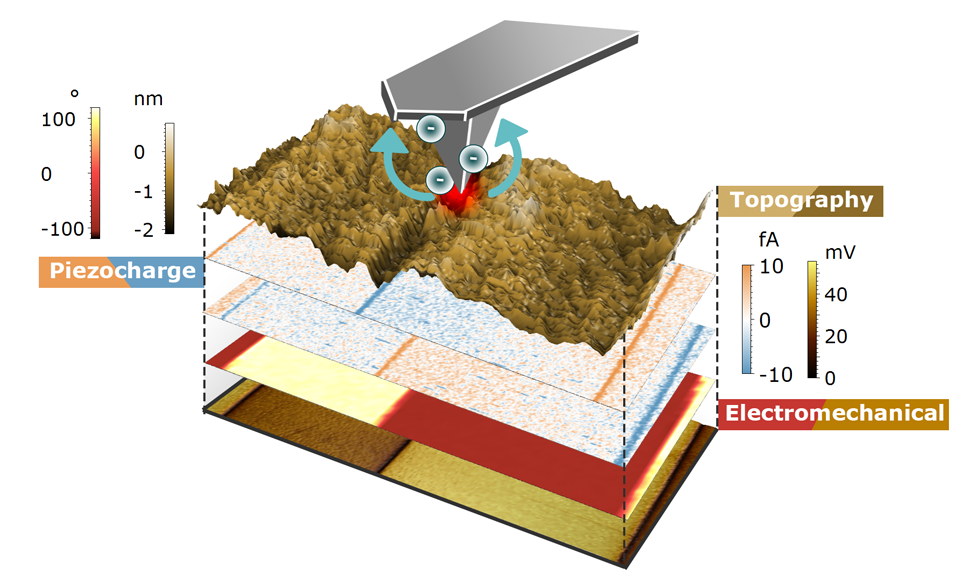
While piezoelectric and ferroelectric materials play a key role in many everyday applications, there are still a number of open questions related to their physics. To enhance our understanding of piezoelectrics and ferroelectrics, nanoscale characterization is essential. Here, we develop an atomic force microscopy based mode that obtains a direct quantitative analysis of the piezoelectric coefficient d33. We report nanoscale images of piezogenerated charge in a thick single crystal of periodically poled lithium niobate (PPLN), a bismuth ferrite (BiFO3) thin film, and lead zirconate titanate (PZT) by applying a force and recording the current produced by these materials. The quantification of d33coefficients for PPLN (14 ± 3 pC per N) and BFO (43 ± 6 pC per N) is in agreement with the values reported in the literature. Even stronger evidence of the reliability of the method is provided by an equally accurate measurement of the significantly larger d33 of PZT.

Competition between Polar and Nonpolar Lattice Distortions in Oxide Quantum Wells: New Critical Thickness at Polar Interfaces

Competition between Polar and Nonpolar Lattice Distortions in Oxide Quantum Wells: New Critical Thickness at Polar Interfaces

J. Gazquez, M. Stengel, R. Mishra, M. Scigaj, M. Varela, M. A. Roldan, J. Fontcuberta, F. Sánchez, and G. Herranz. Phys. Rev. Lett. 119, 106102 – Published 7 September 2017. DOI: https://doi.org/10.1103/PhysRevLett.119.106102

Two basic lattice distortions permeate the structural phase diagram of oxide perovskites: antiferrodistortive (AFD) rotations and tilts of the oxygen octahedral network and polar ferroelectric modes. With some notable exceptions, these two order parameters rarely coexist in a bulk crystal, and understanding their competition is a lively area of active research. Here we demonstrate, by using the LaAlO3/SrTiO3 system as a test case, that quantum confinement can be a viable tool to shift the balance between AFD and polar modes and selectively stabilize one of the two phases. By combining scanning transmission electron microscopy (STEM) and first-principles-based models, we find a crossover between a bulklike LaAlO3 structure where AFD rotations prevail, to a strongly polar state with no AFD tilts at a thickness of approximately three unit cells; therefore, in addition to the celebrated electronic reconstruction, our work unveils a second critical thickness, related not to the electronic properties but to the structural ones. We discuss the implications of these findings, both for the specifics of the LaAlO3/SrTiO3 system and for the general quest towards nanoscale control of material properties.

Probing localized strain in solution-derived YBa2Cu3O7−δ nanocomposite thin films

Roger Guzman, Jaume Gazquez, Bernat Mundet, Mariona Coll, Xavier Obradors, and Teresa Puig. Phys. Rev. Materials. DOI: 10.1103/PhysRevMaterials.1.024801

Enhanced pinning due to nanoscale strain is unique to the high-Tc cuprates, where pairing may be modified with lattice distortion. Therefore a comprehensive understanding of the defect landscape is required for a broad range of applications. However, determining the type and distribution of defects and their associated strain constitutes a critical task, and for this aim, real-space techniques for atomic resolution characterization are necessary. Here, we use scanning transmission electron microscopy (STEM) to study the atomic structure of individual defects of solution-derived YBa2Cu3O7 (YBCO) nanocomposites, where the inclusion of incoherent secondary phase nanoparticles within the YBCO matrix dramatically increases the density of Y1Ba2Cu4O8 (Y124) intergrowths, the commonest defect in YBCO thin films. The formation of the Y124 is found to trigger a concatenation of strain-derived interactions with other defects and the concomitant nucleation of intrinsic defects, which weave a web of randomly distributed nanostrained regions that profoundly transform the vortex-pinning landscape of the YBCO nanocomposite thin films.

Novel Fe3O4@GNF@SiO2 nanocapsules fabricated through the combination of an in situ formation method and SiO2 coating process for magnetic resonance imaging

Novel Fe3O4@GNF@SiO2 nanocapsules fabricated through the combination of an in situformation method and SiO2 coating process for magnetic resonance imaging

Changyong Lu,* Stefania Sandoval, Teresa Puig, Xavier Obradors, Gerard Tobias, Josep Rosa and Susagna Ricart. RSC Adv., 2017, 7, 24690. DOI: 10.1039/c7ra04080f

An in situ approach for the synthesis of Fe3O4 nanoparticles combined with a SiO2 coating process was employed to prepare Fe3O4@GNF@SiO>2 nanocapsules. Graphitised nanofibres (GNF) were initially filled with iron(III) acetylacetonate, and used as a precursor for the synthesis of ultrasmall Fe3O4 nanoparticles (4.6 nm in diameter) inside the cavities of GNF (Fe3O4@GNF) with a high density. By using a silica coating process, Fe3O4@GNF@SiO>2 nanocapsules were obtained. The presence of the silica shell not only prevented leakage of the nanoparticles from inside the GNF but also protected the magnetite nanoparticles from dissolution, even in harsh acidic conditions. Furthermore, the silica coating resulted in an increased dispersability of the nanocomposites in water. Magnetic resonance imaging (MRI) studies indicate relatively high Image ID:c7ra04080f-t1.gif relaxivities for Fe3O4@GNF nanocomposites and Fe3O4@GNF@SiO>2 nanocapsules revealing the potential application of these hybrid materials for bioimaging. Therefore, the coating of filled GNF with silica is as an excellent strategy for the protection of encapsulated payloads.

Institut de Ciència de Materials de Barcelona ICMAB CSIC

Address

Campus de la UAB, 08193 Bellaterra, Barcelona, Spain
+34 935 801 853 ext 371 
hr_suman@icmab.es