Author: Patricia Álvarez

Coated conductors for power applications: materials challenges

sust490440f3_online X.Obradors and T. Puig Molina Supercond. Science & Technology 27, 044003 (2014) DOI:10.1088/0953-2048/27/4/044003 This manuscript reports on the recent progress and the remaining materials challenges in the development of coated conductors (CCs) for power applications and magnets, with a particular emphasis on the different initiatives being active at present in Europe. We first summarize the scientific and technological scope where CCs have been raised as a complex technology product and then we show that there exists still much room for performance improvement. The objectives and CC architectures being explored in the scope of the European project EUROTAPES are widely described and their potential in generating novel breakthroughs emphasized. The overall goal of this project is to create synergy among academic and industrial partners to go well beyond the state of the art in several scientific issues related to CCs’ enhanced performances and to develop nanoengineered CCs with reduced costs, using high throughput manufacturing processes which incorporate quality control tools and so lead to higher yields. Three general application targets are considered which will require different conductor architectures and performances and so the strategy is to combine vacuum and chemical solution deposition approaches to achieve the targeted goals. A few examples of such approaches are described related to defining new conductor architectures and shapes, as well as vortex pinning enhancement through novel paths towards nanostructure generation. Particular emphasis is made on solution chemistry approaches. We also describe the efforts being made in transforming the CCs into assembled conductors and cables which achieve appealing mechanical and electromagnetic performances for power systems. Finally, we briefly mention some outstanding superconducting power application projects being active at present, in Europe and worldwide, to exemplify the strong advances in reaching the demands to integrate them in a new electrical engineering paradigm.

Neutron and X-ray diffraction study of ferrite nanocrystals obtained by microwave-assisted growth. A structural comparison with the thermal synthetic route.

kk5153fig3 E. Solano, C. Frontera, I. Puente Orench, T. Puig, X. Obradors, S. Ricart and J. Ros Journal of Applied Crystallography 47, 1478 (2014) DOI: 10.1107/S1600576714017452 Neutron and X-ray powder diffraction have been used to investigate the differences between the crystal growth of ferrite magnetic nanoparticles (MFe2O4 with M = Mn, Fe, Co, Ni, Zn) by two methodologies: microwave radiation and thermal decomposition routes. Rietveld refinement has been used to extract the cationic distribution, the microstructure and magnetic information. Results for the nanoparticles produced by the two procedures evidence similar cationic distribution, microstructure and magnetic properties: complete cationic disorder for M = Mn and Co, crystal size around/below 10 nm etc. It is thus proven that microwave-assisted growth is a promising eco-friendly synthetic technique for the generation of high-quality nanocrystals with comparable structure and properties to those produced by the thermal methodology, even though the microwave route needs a shorter time and lower annealing temperature to obtain the final crystal nanoparticles.

Ferromagnetic 1D oxide nanostructures grown from chemical solutions in confined geometries

ferromagnetic
Chem. Soc. Rev., 2013
DOI: 10.1039/C3CS60288E
This review summarizes the capabilities and recent developments of nanoporous polymeric template systems directly supported on different substrates for the confined growth of epitaxial ferromagnetic complex oxide 1D nanostructures. In particular, we describe the versatility and potentiality of chemical solutions combined with track-etched polymers to synthesize (i) vertical polycrystalline La0.7Sr0.3MnO3 nanorods on top of single crystal perovskites, (ii) single crystalline manganese based octahedral molecular sieve (OMS) nanowires on silicon substrates, and (iii) the epitaxial directional single crystal OMS nanowires on top of fluorite-type substrates. The influence of the distinct growth parameters on the nanostructural evolution of the resulting nanostructures and their magnetic properties is further discussed in detail.

Magnetic and structural characterization of inkjet-printed TFAYBa2Cu3O7−x/MODCZO/ABADYSZ/SS coated conductors

sust485654f4_online E. Bartolome, R. Vlad, A. Calleja, M. Aklalouch, R. Guzman, J Arbiol, X. Granados, A. Palau, X. Obradors, T. Puig and A. Usokin Superconductor Science and Technology 26, 125004 (2013) DOI:10.1088/0953-2048/26/12/125004 
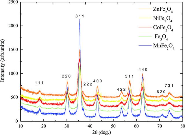
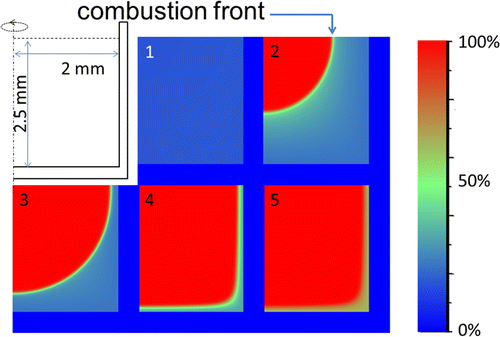
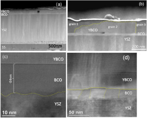
The superconductor industry is demanding new methodologies to manufacture km-long, high quality coated conductors at high growth rates, using cost-effective, scalable processes. We report on the fabrication by an all-chemical deposition method of highly textured, thick (0.9 μm) inkjet-printed YBCO films, using a Ce0.9Zr0.1O2 (CZO) capping layer deposited by MOD, on top of robust, buffered ABADYSZ/SS substrates. Thinner, 0.25 μm spin-coated YBCO films were also analyzed for comparison. The structural study performed by x-ray diffraction, optical, AFM, SEM and TEM microscopy demonstrates the success of the capping layer for enhancing the planarity of the as-received tape and obtaining highly homogeneous and well-textured YBCO films. DC magnetometry granularity analysis was used to determine the mean superconducting grain diameter, ~2.5 μm, and the intra- and intergranular critical current densities of the coated conductors (CCs). For the thin, spin-coated sample, high self-field intragrain critical currents were measured (, 3.3 MA cm−2 at 5, 77 K). For the thick, inkjet-printed tape was reduced by ~30%, but, notably, the percolative critical current, , was only ~10% smaller at 5 K, thanks to good preservation of the texture. At 77 K, was achieved, implying a critical current of Ic = 117 A/cm-width. AC susceptibility measurements allowed us to demonstrate the high homogeneity of the fabricated CCs, and investigate the magnetic vortex-pinning phase diagram. Remarkably, the thick, inkjet-printed sample showed comparable irreversibility line (IL) and activation energy for thermal depinning, Ue(H), to the thin sample. The present results open new perspectives for the fabrication of high quality-to-cost ratio, all-chemical CCs with yet higher Ic values by inkjet printing multideposition of thicker YBCO layers.

Tunable near-infrared and visible-light transmittance in nanocrystal-in-glass composites

nature12398-f1 Anna Llordés, Guillermo Garcia, Jaume Gazquez & Delia J. Milliron Nature 500, 323–326 doi:10.1038/nature12398 Amorphous metal oxides are useful in optical, electronic and electrochemical devices. The bonding arrangement within these glasses largely determines their properties, yet it remains a challenge to manipulate their structures in a controlled manner. Recently, we developed synthetic protocols for incorporating nanocrystals that are covalently bonded into amorphous materials. This ‘nanocrystal-in-glass’ approach not only combines two functional components in one material, but also the covalent link enables us to manipulate the glass structure to change its properties. Here we illustrate the power of this approach by introducing tin-doped indium oxide nanocrystals into niobium oxide glass (NbOx), and realize a new amorphous structure as a consequence of linking it to the nanocrystals. The resulting material demonstrates a previously unrealized optical switching behaviour that will enable the dynamic control of solar radiation transmittance through windows. These transparent films can block near-infrared and visible light selectively and independently by varying the applied electrochemical voltage over a range of 2.5 volts. We also show that the reconstructed NbOx glass has superior properties—its optical contrast is enhanced fivefold and it has excellent electrochemical stability, with 96 per cent of charge capacity retained after 2,000 cycles.

Thermal analysis for low temperature synthesis of oxide thin films from chemical solutions

jp-2013-049742_0006 D. Sanchez-Rodriguez, J. Farjas, P Roura, S. Ricart, N. Mestres Andreu, X. Obradors and T. Puig Journal of Physical Chemistry C 117, 20133-20138 (2013) DOI: 10.1021/jp4049742 The possibility of synthesizing functional oxide thin films at low temperature via combustion synthesis is analyzed both experimentally and numerically. To this aim, the decomposition of several oxide precursors [copper and cerium acetates, yttrium trifluoroacetate, and In2O3 and La0.7Sr0.3MnO3 (LSMO) nitrate based precursors] has been analyzed by thermal analysis techniques. It is shown that, although these precursors decompose via combustion when they are in the form of powders, their corresponding films show no evidence of combustion. The reason for this different behavior is clearly revealed with numerical simulations. Thin films will hardly experience combustion because the precursor front extinguishes before reaching the precursor–substrate interface leaving a “cool zone” hundreds of micrometers thick. In contrast, it is argued that thin oxide films can be obtained at temperatures lower than powders because of the enhanced gas transport mechanisms that usually limit the decomposition rate.

Soft-Chemistry–Based Routes to Epitaxial α-Quartz Thin Films with Tunable Textures

F1.large

A. Carretero-Genevrier, M. Gich, L. Picas, J. Gazquez, G. L. Drisko, C. Boissiere, D. Grosso, J. Rodriguez-Carvajal, C. Sanchez,*

Science 17 May 2013: Vol. 340 no. 6134 pp. 827-831 DOI: 10.1126/science.1232968
Piezoelectric nanostructured quartz films of high resonance frequencies are needed for microelectronic devices; however, synthesis methods have been frustrated by the inhomogeneous crystal growth, crystal twinning, and loss of nanofeatures upon crystallization. We report the epitaxial growth of nanostructured polycrystalline quartz films on silicon [Si(100)] substrates via the solution deposition and gelation of amorphous silica thin films, followed by thermal treatment. Key to the process is the combined use of either a strontium (Sr2+) or barium (Ba2+) catalyst with an amphiphilic molecular template. The silica nanostructure constructed by cooperative self-assembly permits homogeneous distribution of the cations, which are responsible for the crystallization of quartz. The low mismatch between the silicon and α-quartz cell parameters selects this particular polymorph, inducing epitaxial growth.

Photoemission electron microscopy study of sub-200 nm self-assembled La0.7Sr0.3MnO3 epitaxial islands

GA (1) J. Zabaleta, S. Valencia, F. Kronast, C. Moreno, Patricia Abellan, J. Gazquez Alabart, H. Sepehri-Amin, F. Sandiumenge Ortiz, T. Puig Molina, N. Mestres Andreu and X. Obradors Berenguer Nanoscale 5, 2990-2998 (2013) DOI: 10.1039/C3NR33346A The chemical composition and the magnetic structure of individual La0.7Sr0.3MnO3 (LSMO) ferromagnetic manganite epitaxial nanostructures less than 200 nm in width are explored using Photoemission Electron Microscopy (PEEM). X-ray absorption spectra (XAS) provide separate information on the surface and the bulk composition of the nanoislands and give evidence of Mn2+ present on the surface of otherwise stoichiometric nanostructures. Ferromagnetic domains less than 70 nm are resolved using X-ray magnetic circular dichroism (XMCD), which allows for the detection of magnetic vortex states in both (001)LSMO square and (111)LSMO triangular manganite nanoislands. The evolution of single nanostructures under an in-plane magnetic field is seen to depend on the specific nanoisland size and geometry. In particular, PEEM XMCD imaging allows detecting opposite chiralities as well as a variety of magnetization behaviors for different nanoislands.

Strain-driven broken twin boundary coherence in YBa2Cu3O7−δ nanocomposite thin films

1.4793749.online.f2_thmb R. Guzman, J. Gazquez, V. Rouco, A. Palau, C. Magen, M. Varela, J. Arbiol, X Obradors and T. Puig Appl. Phys. Lett. 102, 081906 (2013) http://dx.doi.org/10.1063/1.4793749 In this letter we use high resolution scanning transmission electron microscopy to study epitaxial YBa2 Cu 3O7−δ (YBCO) nanocomposite thin films. We find that twin boundaries (TB) in YBCOnanocomposite thin films are disturbed by the presence of secondary phase nanoparticles as well as by intergrowths. Secondary phases promote the nucleation of TBs and, at the same time, result in bending, decreasing and changing the TB’s spacing. On the other hand, the local strain ensuing from the partial dislocation associated to Y248 and Y125 intergrowths break the verticalcoherence of TBs. This interaction results in a complex domain structure where twin boundarycoherence is no longer satisfied and twin spacing is reduced down to a few nanometers precluding vortex channeling at low temperatures.

Institut de Ciència de Materials de Barcelona ICMAB CSIC

Address

Campus de la UAB, 08193 Bellaterra, Barcelona, Spain
+34 935 801 853 ext 371 
hr_suman@icmab.es